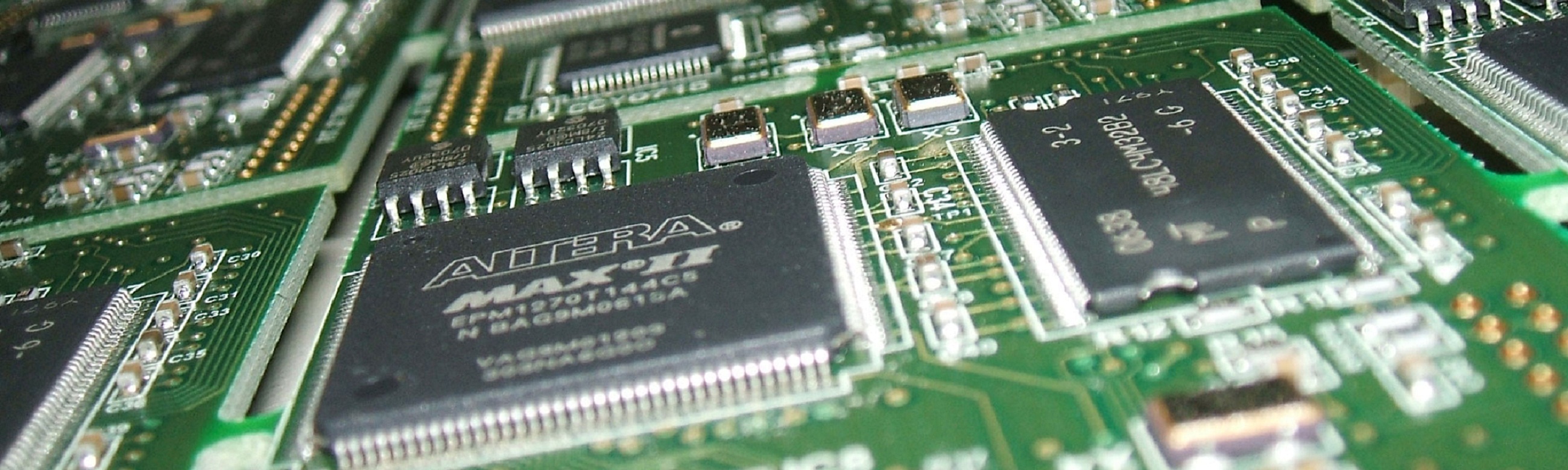
- PCB fabrication up to 60 layers
- Board thickness ranging from 0.015” to 0.500”
- Copper weight from 12 microns (3/8 oz.) to 343 microns (10 oz.)
- Panel sizes up to 31” x 52”
- Support for large form factor and high-aspect ratio backplanes
- Embedded passives (ZBC™, Buried Capacitance®, Annular Buried Resistance technologies)
- Use of high-performance materials and composites
- Signal-integrity modeling for enhanced performance
- High-speed 10 Gbps capability through innovative engineering
- Fabrication of Rigid-Flex-Rigid Boards
The ability to perform signal integrity analysis, electromagnetic compliance (EMC) analysis, and crosstalk analysis early in the product development process is essential to successful High-Speed PCB designs, particularly as IC switching and clock speeds escalate. Pre- and post-layout signal integrity EMC and Crosstalk analysis to eliminate issues early in the design process. Locating and solving potential EMC problems early in your design process is significantly less expensive than fixing problems at the prototype stage.
We have expertise in handling printed circuit board design services for mixed signal, high-speed digital and analog power boards, setting us apart from our competitors. Our PCB layout services involve the use of highly efficient PCB design tools for innovative printed circuit board design using custom scripts and programs to increase efficiency, augment the current design tools, and improve quality.
PCB Design And Layout Expertise:
We can handle almost all PCB services including designs, layouts, and prototyping. We use the most recent and updated design software to develop the most seamless design. By outsourcing PCB design services to India, you can be assured of
- High-speed Printed Circuit Board design with unmatched quality.
- Handling boards that are single-sided as well as multi-layered.
- Placement of the components just the way customer demands.
- Giving extreme care on route trace.
- Creating footprints for special packages.
- Getting layout services for new printed circuit boards and also for existing boards that require changes.
- Application of various tests to avoid issues that can occur during the manufacturing process.