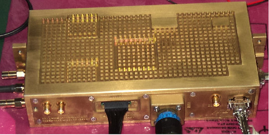
The system shall take Analog signals from different channels and process through LNA, DVGA chip to meet accurate signal gain. The processed signal is sent to Digital Down conversion chip it has a front end ADC and converted data is processed with different filters available in the DDC chip. The filtered data of 16 bit data is sent through I & Q channels. The DDC chip interface and control with FPGA.
The DAC’s are interfaced with FPGA and DDC outputs of I & Q channels are sent via DAC’s. This system uses on board clock for all functional operations. There is also an external clock through jumper where the on board clock will disable and external clock activated and performs all functional operations.
- The signal and data processing unit is configured around one FPGA and two Tiger Sharc DSP processors.
- The DSP Processor supports up to 600MHz, 1ns instruction cycle rate
- The DSP processor has 24Mbits On-Chip-DRAM memory
- All Signal processing algorithms will be running in DSP
- The system Communicates through MIL 1553 and RS422
- The MIL1553 have high speed data communication
- All other communications are implemented with RS422
- Processor: Two Tiger SHARC (ADSP-TS201SABP-060)@600MHz
- FPGA: One Xilinx VERTEX 5 (XC5VLX50-FF1153)
- FPGA PROM: XCF16PV048C
- Boot Flash: capacity : 512K x 8Bits,FLASH Part No : AT49BV040B-JU,Number of ICs used : 01
- Application Flash: Capacity : 512K x 8 Bits
- FLASH Part No : AT49BV040B-JU, Capacity : 512K x 8,Number of ICs used : 01
- DDC: No. of Channels : 3,Input Power range : -110 dBm to -10dBm
- DDC Part No.AD6654CBCZ,DDC resolution : 14 bit,CONNECTORS TYPE: SMA
- FLAGS: 4,Software configurable as input or output in DSP
- RESET OPTIONS Required 1. Software reset.,2. Power ON reset.,3. Manual reset.
